Si Wet Etching Simulator
3D anisotropic/isotropic wet etching simulation for single-crystal (100) silicon
Open the simulator or download the example DXF mask file:
▶ Launch Simulator
The example DXF (SiEtchTestmm.dxf) contains a substrate outline on layer
0 and several mask patterns — including axis-aligned rectangles and a 45°-rotated
diamond — on layer mask, all in millimeters.
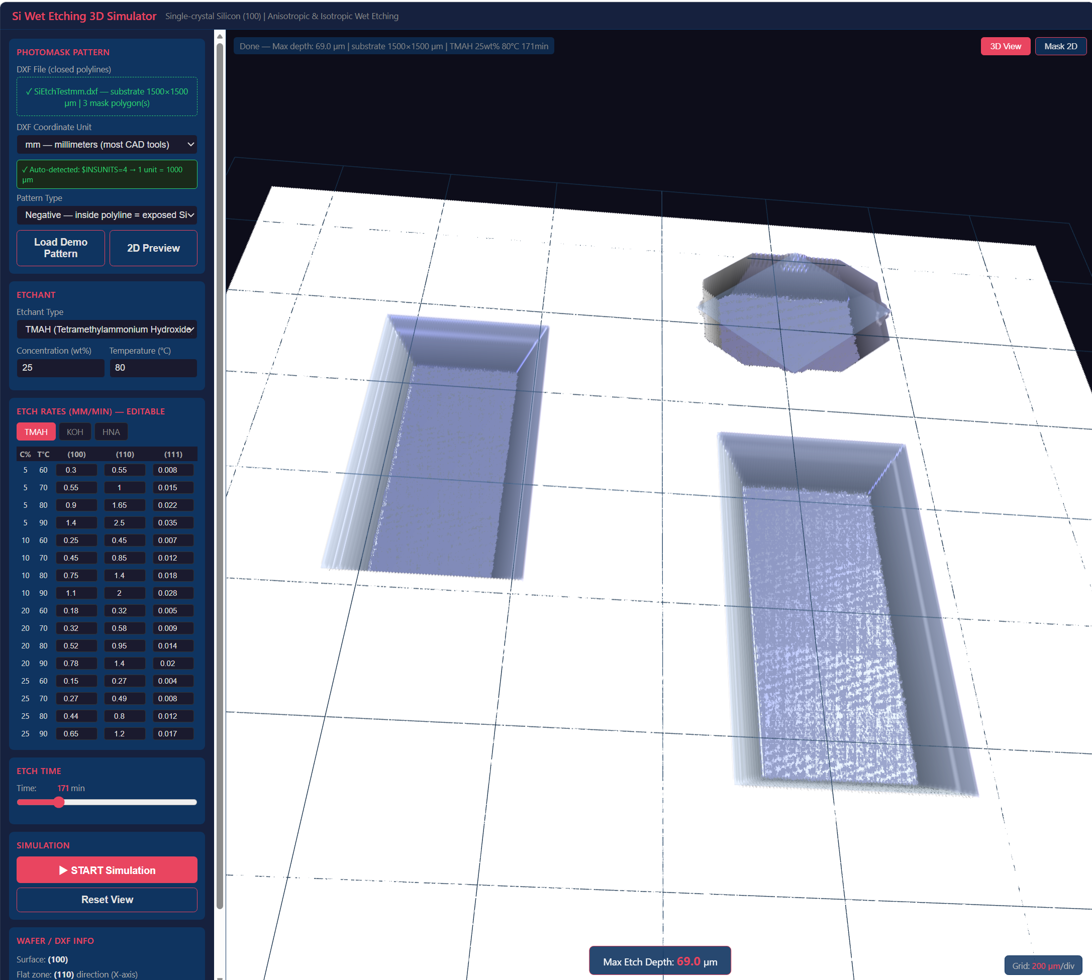 Fig. 1 Simulator interface: parameter panel (left), Etch mask pattern or etched 3D shape (right).
1. Overview
This tool simulates the three-dimensional etch profile produced when a patterned (100)-oriented single-crystal silicon wafer is immersed in a wet chemical etchant. Given a mask layout (DXF), an etchant type and concentration, a temperature, and an etch time, the simulator computes and renders the resulting 3D cavity shape interactively in the browser — no installation required.
Wafer orientation convention used throughout: the X-axis is parallel to the [110] crystal direction (i.e. aligned with the primary flat of a standard (100) wafer). The Y-axis is [1̅10]. All mask coordinates in the DXF file should follow this convention.
2. Physical Model
2.1 Continuous Cellular Automata (CA)
The simulation engine is based on the continuous cellular automata method described in:
Zhu, Z. and Liu, C. (2000). "Simulation of anisotropic crystalline etching using a continuous cellular automata algorithm." CMES: Computer Modeling in Engineering & Sciences, 1(1), pp. 11–19.
The silicon substrate is represented as a 3-D array of voxels. Each voxel carries a continuous mass variable M ∈ [0, 1], where 1 = intact silicon and 0 = fully etched. Only voxels at the silicon–etchant interface (the active surface) are processed at each time step; interior and masked voxels are skipped, keeping computation efficient.
At every time step each active voxel inspects its four tetrahedral neighbors (following the diamond-cubic silicon lattice) and is classified as one of three surface types:
| Neighbor pattern | Surface type | Etch rate used |
|---|---|---|
| 2 etched, 2 solid | {100} | R100 — fastest |
| 1 etched, 1 solid, 2 surface | {110} | R110 |
| 1 etched, 3 solid | {111} | R111 — near zero (etch stop) |
The mass of a voxel is reduced by rate × dt / GRID_RES each step.
When M reaches 0 the voxel is removed and its neighbors are promoted to the active surface.
This allows the {111} etch-stop planes to form naturally without any hard-coded geometry.
2.2 Coordinate rotation
Because the CA neighbor vectors are defined in the crystal [100]/[010]/[001] frame, the mask input is internally rotated +45° into crystal coordinates before the simulation runs, and the resulting height-field mesh is rotated −45° back for display. The substrate outline and mask layer rendered on screen always match the original CAD coordinates.
2.3 HNA (isotropic) etching
HNA (HF + HNO₃ + CH₃COOH) etches silicon isotropically. In this mode all surface types receive the same etch rate, producing hemispherical undercut profiles. Published etch-rate data for HNA is only reliable near room temperature, so the temperature selector is restricted to 15–30 °C for this etchant.
3. Interface
The window is split into a left panel (inputs) and a right viewport (graphics).
Left panel — input sections
| Section | Key points |
|---|---|
| Photomask Pattern |
Upload a DXF file or click Load Demo Pattern to use a built-in test layout.
Choose Positive (polyline interior = masked) or
Negative (polyline interior = exposed silicon).
The 2D Preview button switches the viewport to a top-down mask view
with pan and zoom.
The DXF coordinate unit is auto-detected from $INSUNITS; if absent,
select the correct unit manually from the dropdown.
|
| Etchant | Choose TMAH, KOH, or HNA. Enter concentration (wt%) and temperature. Temperature range is limited to 15–30 °C for HNA. |
| Etch Rates (editable table) | Shows interpolated etch rates (µm/min) for {100}, {110}, and {111} planes at several concentration/temperature combinations from the literature. Values are editable — useful for calibrating to your own process data. Switch between etchant tabs to inspect or edit rates for each chemistry. |
| Etch Time | Slider, 1–800 minutes. |
| Simulation | Click START Simulation to run. A progress bar shows CA stepping. The grid resolution (GRID_RES) is chosen automatically to keep the voxel count near 20 million; if a finer grid is used, the resolution remains at the 2 µm base; if the domain or etch depth is large the step is coarsened and a notice is shown. |
Right viewport — 3D view
- Rotate — left-click and drag.
- Pan — right-click and drag.
- Zoom — scroll wheel.
- Reset View button — returns camera to the default position.
- The mask layer is rendered semi-transparent in blue, so the etched silicon underneath is visible.
- Max etch depth (µm) is displayed at the bottom-centre of the viewport after a simulation completes.
- The 3D / Mask 2D toggle in the top-right corner switches between the three-dimensional result and the 2D mask preview.
- A grid is drawn on the wafer plane with a division size chosen to give roughly 10 lines across the substrate. The scale (n µm/div) is shown at the bottom-right of the viewport.
4. DXF Input Format
Save your mask file as DXF R2000 (AutoCAD 2000) or later. The file must contain closed polylines on two specific layers:
| Layer name | Contents | Usage |
|---|---|---|
0 |
One closed rectangle defining the silicon substrate boundary | Sets the simulation domain. The largest-area polygon on this layer is used. |
mask |
One or more closed polylines defining the mask pattern | Positive or negative, depending on the Pattern Type selection. |
The recommended coordinate unit is millimeters (set $INSUNITS = 4
in the DXF header, which most CAD tools do automatically when saving in mm).
Other units (µm, cm, m, inch) are also supported via the unit dropdown; the
$INSUNITS header value is read first and the dropdown is set accordingly,
with a warning if the header is absent.
Polylines that are neither LWPOLYLINE nor POLYLINE entities, and any entities on layers
other than 0 and mask, are ignored.
5. Etchants and Etch-Rate Tables
Default etch-rate values in the editable tables are taken from published literature (Tabata 1992, Seidel 1990, Zubel 2001 for TMAH/KOH; manufacturer data for HNA) and interpolated bilinearly in concentration and temperature. Values for intermediate concentrations/temperatures not listed in the table are obtained by bilinear interpolation between the nearest entries.
| Etchant | Typical use | Selectivity R₁₀₀:R₁₁₀:R₁₁₁ | Temperature range |
|---|---|---|---|
| TMAH | CMOS-compatible, no metal contamination | ~1 : 1.8 : 0.02 | 60–90 °C |
| KOH | High etch rate, most common | ~1 : 2 : 0.01 | 50–90 °C |
| HNA | Isotropic; rounded cavities | 1 : 1 : 1 | 15–30 °C |
6. Typical Workflow
-
Prepare a DXF file with the substrate rectangle on layer
0and mask openings on layermask, saved in mm (R2000 format). Alternatively, click Load Demo Pattern to start immediately. - Drag-and-drop (or click to browse) the DXF into the Photomask Pattern area. Verify the auto-detected unit and substrate size in the status bar, then click 2D Preview to confirm the mask layout.
- Select the etchant, enter concentration and temperature. Optionally inspect and edit etch rates in the table.
- Set etch time with the slider.
- Click START Simulation. Wait for the progress bar to complete (seconds to a few minutes depending on domain size and etch time).
- Rotate, pan, and zoom the 3D result. Check the maximum etch depth displayed at the bottom of the viewport. Adjust time or etchant parameters and re-run as needed.
7. Limitations and Known Constraints
- Grid resolution adapts to domain size. The base voxel size is 2 µm; for large substrates or long etch times the simulator automatically coarsens the grid (up to 20 µm/voxel) to keep the total voxel count near 20 million. Very large domains (> 10 mm side) combined with long etch times may not be simulatable at useful accuracy.
- Only (100) surface orientation is supported. The CA neighbor geometry and the coordinate-rotation trick are specific to (100) wafers with the primary flat along [110].
- Convex-corner undercut at high-index planes ({211}, {311}, etc.) is not explicitly modeled. The CA rules cover only {100}, {110}, and {111}. In practice, convex corners are slightly over-retained compared with experiment.
- HNA temperature range is restricted to 15–30 °C because reliable published data outside that range is not available; the simulator does not extrapolate.
- Mask material is ideal. Real masks (SiO₂, Si₃N₄, photoresist) have finite etch rates and may pin-hole; this is not modeled.
- No etchant depletion, stirring, or temperature gradients are modeled. The simulation assumes a uniform, well-mixed etchant bath at steady state.
- The tool runs entirely in the browser (JavaScript / WebGL via Three.js). No data is sent to any server.
Simulator built with Three.js (r128) for 3D rendering and a custom continuous-CA engine in plain JavaScript. DXF parsing handles LWPOLYLINE and POLYLINE entities. Default etch-rate data from open literature; all values are editable in the UI.