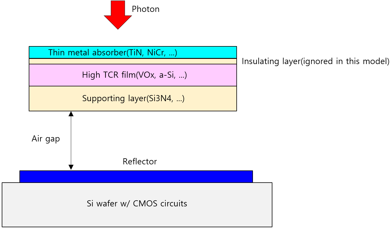
Fig. 1 — Structure of IR absorber
▶ Open IR Absorption Calculator
This web tool calculates the normal-incidence infrared (IR) absorption spectrum of a bolometer-type thermal imager pixel as a function of wavelength (1–10 μm). The pixel is modeled as a multilayer thin-film stack sitting above a silicon substrate. Given the layer thicknesses and material parameters, the tool returns the spectral absorptance A(λ), reflectance R(λ), and transmittance T(λ) across the chosen wavelength range.
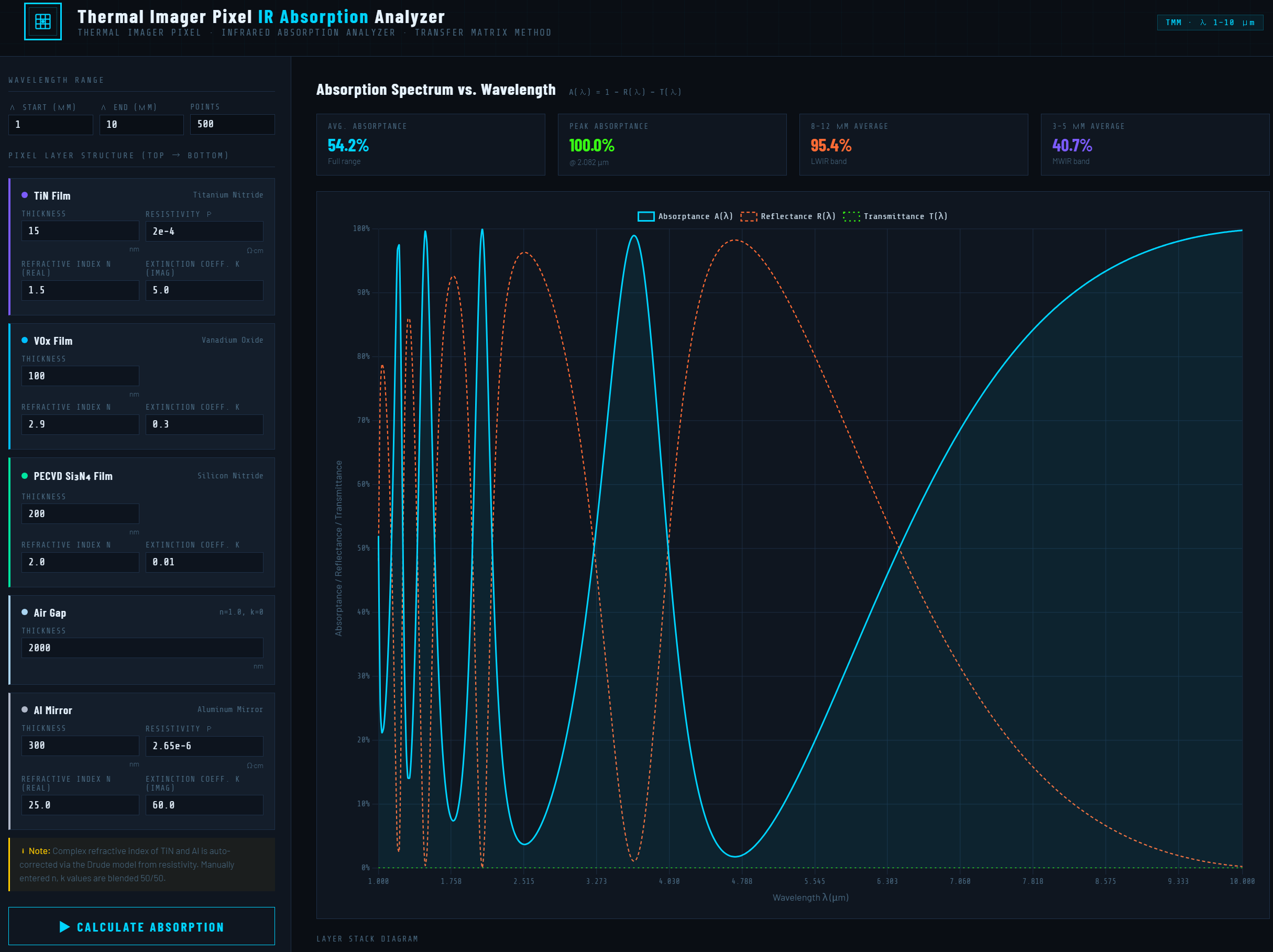
The left panel contains all input parameters. After adjusting the values, click "▶ 흡수도 계산" (Calculate Absorption) to update the chart. The right panel displays the computed spectra and four summary statistics (overall average, peak absorption wavelength, LWIR 8–12 μm average, and MWIR 3–5 μm average).
The pixel structure is a five-layer stack on top of a semi-infinite silicon substrate. Layers are ordered from the IR-incident surface downward:
| # | Layer | Role | Default thickness | Optical model |
|---|---|---|---|---|
| 1 | TiN | Absorbing top electrode / IR absorber | 15 nm | Drude + user n, k (blended) |
| 2 | VOx | Thermistor (resistive sensing) layer | 100 nm | Complex refractive index n, k |
| 3 | PECVD Si3N4 | Structural membrane / IR-transparent support | 200 nm | n, k + phonon absorption correction (∼11.5 μm and ∼13 μm bands) |
| 4 | Air gap | Cavity spacer (quarter-wave resonator) | 2000 nm | n = 1, k = 0 (fixed) |
| 5 | Al mirror | Back reflector | 300 nm | Drude + user n, k (blended) |
The incident medium is air (n = 1); the substrate is treated as semi-infinite silicon (n = 3.4, k = 0).
The spectral response is computed using the Transfer Matrix Method, a standard analytical technique for plane-wave propagation through planar multilayer stacks (Born & Wolf, Principles of Optics, Ch. 1). For each wavelength λ, a 2×2 characteristic matrix is computed for every layer and the matrices are multiplied together to yield the total stack matrix, from which Fresnel reflection and transmission amplitudes are derived.
The characteristic matrix for layer j with complex refractive index
ñj = nj + i kj
and thickness dj is:
Absorptance is then obtained from energy conservation:
For the metallic layers (TiN and Al), the complex permittivity is partially derived from the Drude free-electron model using the DC resistivity ρ entered by the user:
Default relaxation times: TiN τ = 4×10⁻¹⁵ s, Al τ = 8×10⁻¹⁵ s. The Drude result is blended 50/50 with the manually entered n, k values.
PECVD silicon nitride exhibits strong phonon absorption bands in the LWIR range. Two Gaussian correction terms are added to the user-supplied k value: a primary band centered at 11.5 μm (σ = 1.0 μm) and a secondary band at 13.0 μm (σ = 0.5 μm).
All inputs have physically reasonable default values pre-filled. Users familiar with thin-film optics will recognize the parameter names directly in the interface; only a few points are worth highlighting:
d ≈ λ0 / 4 (e.g., 2500 nm for λ0 = 10 μm).
The chart on the right plots three curves simultaneously:
Hovering over the chart shows precise values at a given wavelength. The four stat boxes above the chart give a quick summary of key figures of merit for LWIR (8–12 μm) and MWIR (3–5 μm) imaging bands.